
Size and weight
Multi-element assemblies place a disproportionate burden on airborne, autonomous, wearable, robotic, and distributed sensing platforms.
Meta-optics for Compact and Scalable Photonics
Coherent Photonics develops innovative photonics solutions based on disruptive, scalable, cost-effective, and compact architectures.
The Optical System Constraint
Sensing and imaging systems often depend on multiple refractive lenses, mirrors, spacers, mechanical housings, precision alignment steps, and relatively large detector areas. Each additional element carries consequences beyond optical performance.
Multi-element assemblies place a disproportionate burden on airborne, autonomous, wearable, robotic, and distributed sensing platforms.
Multiple optical surfaces require precision assembly and tight mechanical tolerances, increasing both cost and integration effort.
Vibration, shock, thermal drift, and long-term mechanical changes can shift alignment and degrade system performance.
Complex optical assemblies are difficult to translate into resilient, high-volume, wafer-compatible production.
Small changes in surface shape may result in significant wavefront errors affecting system performance.
Product variants may require custom optical components followed by renewed mechanical integration and alignment.
Platform
Coherent Photonics develops compact, scalable metasurface components and metasurface sensors supported by physics-informed design, fabrication-aware optimization, and internal prototype characterization.

Five issued U.S. patents, 12 foundational U.S. patent applications and internal know-how.
Computationally efficient, physics-informed AI/ML optimization with design-for-manufacturing.
Internal nanophotonic performance testing and prototype characterization capability.
Device layouts are developed for process runs with established nanophotonics fabricators.
Design Methods
Coherent Photonics works across the development cycle—from conceptual definition and detailed design through tolerance analysis, characterization, and fabrication support.
Coherent Field Transformations
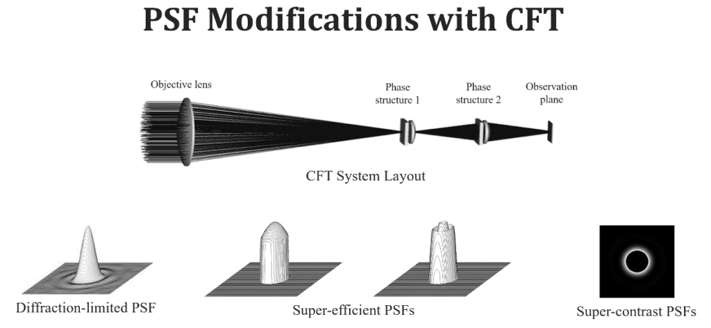
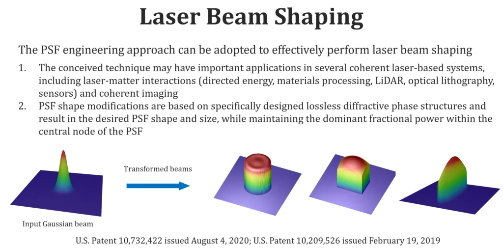
Coherent Field Transformations form optical fields with specified spatial properties and provide direct control over focal-spot shape, size, and point-spread function.
Metasurface Components
Product Concepts
A computational toolset for designing efficient, high-numerical-aperture meta-optics.
Meta-optical polarization-converting and polarizing structures based on engineered ensembles of nano-atoms.
Low-profile, scalable wafer-level components for sensing, imaging, industrial, defense, and advanced photonics systems.
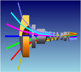
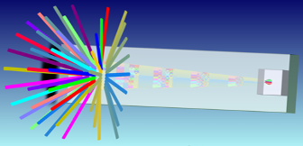
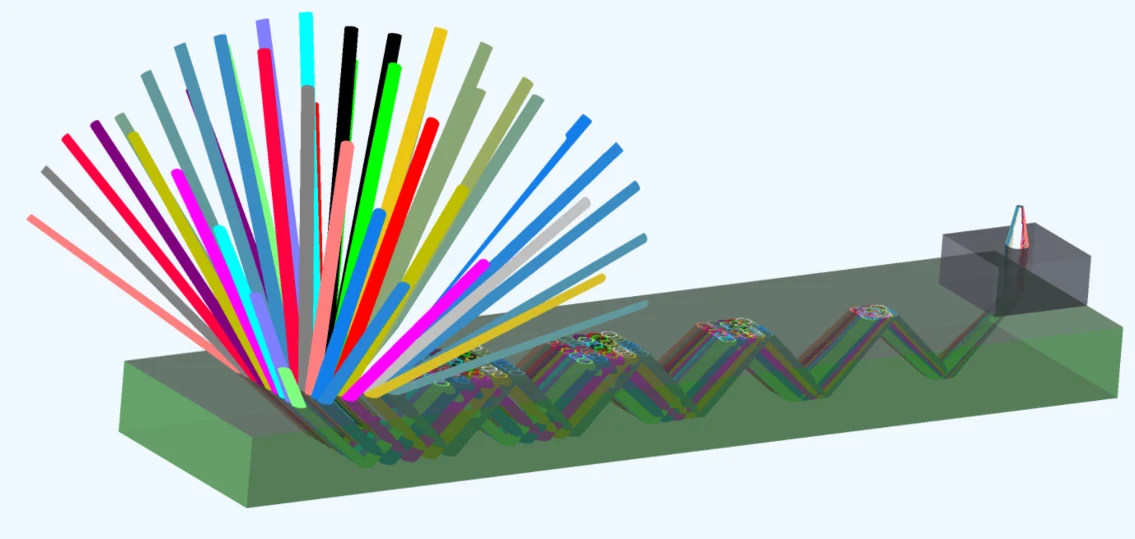
A metasurface monocentric systems architecture for extra-wide-field-of-view panoramic sensing modules.
Applications
A common meta-optics platform supports different applications and products across a variety of operating wavelengths.
Pixel-level meta-optics combine tailored illumination, multiband routing, polarization sorting, and point-spread-function control in compact sensing formats.
Non-mechanical beam steering/shaping with OPA and coherent field transformation concepts for agile optical control.
Beam combining and compensation of atmospheric perturbations complement directional links, multibeam operation, and tunable beam control.
Components and subsystems for high-power optical paths with scalable inorganic material platforms.
Passive components address compact routing and packaging needs; the same architecture extends toward optical switches, routers, and reconfigurable interconnect fabrics.
Intelligent multi-beam scanning supports compact sensing, illumination, and directional optical control for robotics, drones, and autonomous platforms.
Select an option to update the overview and image.
Meta-optics beam-shaping components can address defined laser specifications before integration into compact illumination and scanning modules.
Reduces dependence on difficult-to-procure IR materials by moving to scalable silicon-centric fabrication paths.
Wafer-bonded monolithic options for robust systems with lower alignment burden than free-space assemblies.
Architectures can be tailored across visible and IR ranges and adapted for multiple application modalities.
Beam number, directionality, and peak power can be actively tuned through phase-controlled designs.
Contact Us